III-V ICP Compound Semiconductor Etch System
Service Line: 02 Material Deposition and Etching
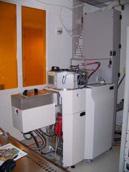
III-V ICP Compound Semiconductor Etch System
The Surface Technology System (STS) Inductively Coupled Plasma (ICP) etch system uses chlorine based chemistry to anisotropically etch substrate materials. The STS ICP etch system is configured to etch compound semiconductor materials such as GaAs, GaN, InP, GaP, and SIC. The STS system provides high rate, high selectivity, and very uniform anisotropic etching of thin film materials.
ICP etch systems employ two RF power supplies. One is capacitively coupled to the electrode while the other is inductively coupled through the walls of the process chamber. ICP etch systems introduce their power into the reactor chamber through this inductively coupled or secondary source. This allows increased plasma power to be introduced without coupling it through the sample. Therefore, ICP etch systems have lower sputtering and operating temperature, reduced charge damage, higher etch rate, and greater etch selectivity. Etching is accomplished through multiple means: (a) chemical adsorption of reactive molecules (free radicals) on the surface; (b) the impact of ions on the surface (reactive or not); (c) the physical disassociation of many reaction by-products from the surface.
Manufacturer: STS
Model:
Contact:
Scott Williams
704-687-8126
scotwill@charlotte.edu
Tool Location:
Grigg Hall, Third Floor Room: CleanRoom Bay Number: 4