JEOL SEM w/EDAX
Service Line: 04 Imaging and Characterization
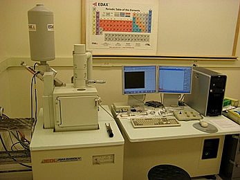
JEOL SEM (Scanning Electron Microscope) w/EDAX
The scanning electron microscope (SEM) is a type of electron microscope that images the sample surface by scanning it with a high-energy beam of electrons in a raster scan pattern. The electrons interact with the atoms that make up the sample producing signals that contain information about the sample’s surface topography and composition.
Maximum Magnification: X300,000
Resolution: 3 nm
Capable of both high and low vacuum operation
Acceleration Voltages: 0.3 Kv to 30 Kv
Current work with the JEOL SEM and EDAX includes:
Imaging of etched micro-lenses as well as other micro and nano-structures.
Imaging and EDS analysis of man-made microspheres, nano–wires, etc.
Imaging and EDS analysis of fossil fuel power plant by-products.
Imaging of surface morphology and EDS analysis of semiconductor thin films.
Manufacturer: JEOL
Model: 6460LV
Contact:
Lou Deguzman
704-687-8111
pcdeguzm@charlotte.edu
Tool Location:
Grigg Hall, First Floor Room: 152 Bay Number: N/A