Capabilities
Etching
Deposition
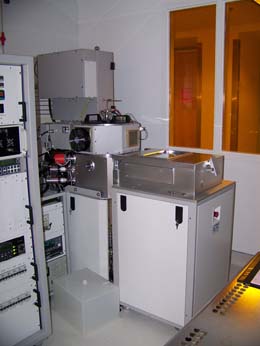
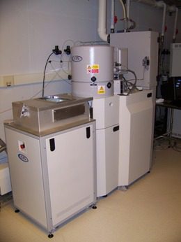
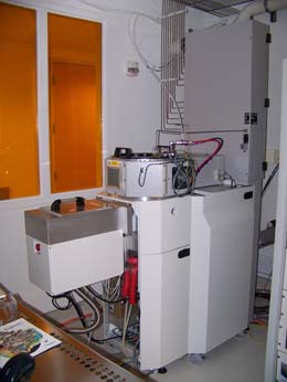
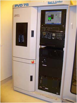
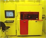
The tool provides thin film metal deposition by electron-beam and thermal evaporation techniques, and has the capacity to process three 100 mm wafers or a single 150, 200, or 300 mm wafer. For various types of thin film structures the AJA International ATC 1800-F Sputter Deposition system is in use as well.
Photolithography
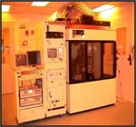
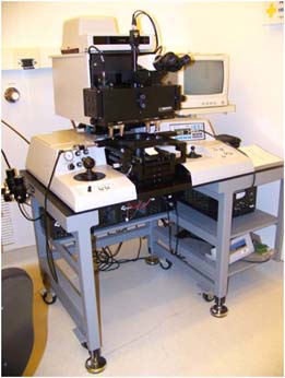
The GCA 5X Stepper, pictured (reduction step and repeat) projection system uses an exposure wavelength of 436 nm (g-line) lens column to provide a 5:1 reduction with a variable field size up to 15mm square. Wafer sizes of 3″ up to 150mm, as well as smaller pieces, can be accepted.
Nano-imprint Lithography
Molecular Imprints’ Imprio 100™ is a nanoreplication tool based on Step and Flash Imprint Lithography delivers high-resolution, sub-micron alignment, and 3-dimensional replication to sub-50nm lithography. Only the template fabrication process, typically with an e-beam writer, limits feature resolution.
Optoelectronic Fabrication and Packaging
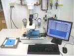
Various types of the COS (“chip-on-submount”) optoelectronic components can be fabricated for prototyping purpose by the following tools: Microautomation Dicing Saw, Loomis LSD-100 Scriber & Breaker (pictured), Finetech Lambda Flip-Chip Die Bonder , K&S 4524AD Wire Bonder.
Characterization and imaging
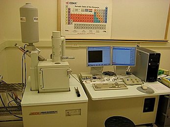
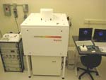
Interferometry, AFM, JEOL SEM (pictured), ellipsometry, Circular dicroism.
Numerical modeling

COMSOL, RSoft, CST Microwave Suite, custom MatLab simulations.
